The Digital I/O Handbook – Chapter 1
The Digital I/O Handbook
A Practical Guide to Industrial Input and Output Applications
Digital I/O Explained
Renowned technical author Jon Titus and the President and CEO of Sealevel Systems, Tom O’Hanlan, clearly explain real-world digital input/output implementation from both a hardware and software perspective. Whether you are a practicing engineer or a student, The Digital I/O Handbook will provide helpful insight you will use again and again.
- Covers a wide range of devices including optically isolated inputs, relays, and sensors
- Shows many helpful circuit diagrams and drawings
- Includes software code examples
- Presents common problems and solutions
- Detailed glossary of common industry terms
“What I like most is its mix of hardware and software. Most pages have a bit of code plus a schematic. All code snippets are in C. This is a great introduction to the tough subject of tying a computer to the real world. It’s the sort of quick-start of real value to people with no experience in the field.” – Jack Ganssle, The Embedded Muse, January, 2005.
You can purchase the Digital I/O Handbook for $19.95 by clicking here. The Digital I/O Handbook is FREE with any qualifying Sealevel Digital I/O product purchase.
Chapter 1 – Logic Principles
Topics Covered
- Introduction to digital electronics
- Current sinks and sources
- Buffers and drivers
- Latches
- Positive and negative logic
- Logic families
Introduction to digital electronics
The world of digital electronics allows for only two states, so at a given time, a digital signal can exist in only one of them. Although engineers usually think of these two binary states as logic 0 and logic 1, you can define them as you wish: true and false, black and white, high and low, and so on, as long as everyone else understands your definitions.
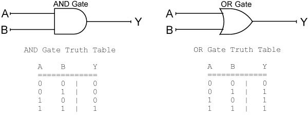
Basic Boolean1 logic operations such as AND and OR let electronic circuits make decisions, such as, “If A and B are true, do this…” Figure 1-1 shows the AND and OR logic operations along with the symbol engineers use to represents each operation in a circuit. A truth table shows the output condition produced for each possible set of inputs to the logic circuit, called a “gate.” A 2-input gate, for example, has 22, or 4 possible input conditions, while a 5-input gate would allow for 25, or 32 possible binary input combinations.
Figure 1-1
Basic AND and OR logic operations follow a set of rules described using truth tables. Even if you substitute “YES” for 1 and “NO” for 0, the rules remain the same.
Note that a 2-input AND gate produces a logic 1 at its output only when a logic 1 exists at input A and at input B. A 2-input OR gate produces a logic 1 when either input A or input B exist in a logic-1 state. On the other hand, when both OR gate inputs change to logic 0, the gate produces a logic 0.
These conditions hold, no matter how many inputs an AND gate or an OR gate has:
- An AND gate puts out a logic 1 only when ALL its inputs exist in the logic-1 state.
- An OR gate puts out a logic 0 only when ALL its inputs exist in the logic-0 state.
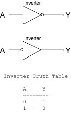
The inclusion of a third logic operation, inversion, completes the family of fundamental logic functions. In Boolean logic, the inversion function goes by the formal name NOT. An inversion operation simply “inverts” a logic 1 to a logic 0, and vice versa, as shown in Figure 1-2. The small circle at the input (flat side) or at the output (apex) of the triangle symbol represents the inversion operation.
Figure 1-2
An inverter simply reverses the logic state of its single input, as shown in the truth table. Inverters appear as small triangles in schematic diagrams and most designers favor drawing the small circle on the output.
So, if a device produces a logic 1 to cause an action, but your circuit requires a logic 0, use an inverter. Likewise, an inverter will change a logic 0 into a logic 1.
Digital circuits may include many discrete inverters, as shown in Figure 1-2. Many schematic diagrams also show an inversion by attaching a small circle to an input or output. But these small circles do not exist on their own in circuit diagrams; youll always see them attached to another symbol.
Combinations of AND, OR, and NOT functions form the basis for all digital electronic circuits. Many circuits combine AND, OR, and NOT functions to form NOT-AND and NOT-OR circuits. Engineers have adopted the names NAND and NOR for these common functions, shown in Figure 1-3. NAND and NOR gates exist in real circuits.
Figure 1-3
Combining AND and OR gates with an inverter function leads to NAND and NOR gates. You can build any digital circuit from these versatile devices.
Combining NAND and NOR gates lets circuit designers produce any digital function. Even the latest microprocessor chips rely on large arrays of these fundamental digital circuits.
In the world of digital electronics, logic 1 and logic 0 correspond to voltages. In the popular family of SN7400-series transistor-transistor logic (TTL) integrated circuits (ICs), a voltage close to 5V represents a logic 1, and a voltage close to 0V, or ground, represents a logic 0. Note that a logic 0 does not mean “nothing” or “unconnected.” Voltages that represent a logic 1 and logic 0 may vary from one family of logic ICs to another, but designers always consider a logic 1 as the higher of the two voltages. For the sake of simplicity, well continue to use the 5V TTL levels in our examples.
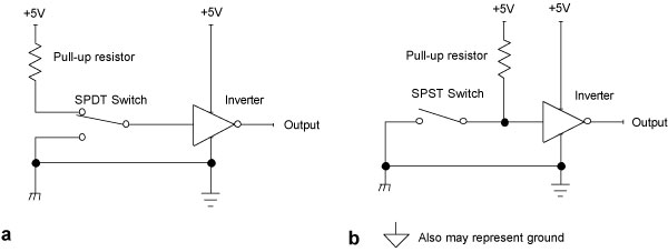
A simple single-pole double-throw (SPDT) switch can easily switch between 5V DC and ground to produce either a logic 1 or a logic 0 at an input to a TTL IC, as shown in Figure 1-4a. Note that the “logic 1” side of the switch connects to the 5V power source through a pull-up resistor. This resistor limits current through the circuit and offers some protection against an inadvertent short circuit, which could damage logic devices.
Figure 1-4
An SPDT switch (a) can change the logic state of an inverters input, but the circuit in (b), provides a better alternative. Note the common ground connection between the inverter and the switch circuit.
Unfortunately, the SPDT switch circuit can cause a problem. Actuating the switch moves a contact between the 5V and GND terminals. During the movement, the contact experiences a short “dead time,” when it touches neither 5V nor GND. In many circuits, this brief time between terminals wouldnt cause a problem. But in a digital circuit it means the input to a device will briefly “float,” which can cause an input to “see” an undetermined state. That condition should not exist in a digital circuit because it can lead to unexpected results.
To avoid this type of problem, use the circuit shown in Figure 1-4b, which eliminates the switchs “dead” time. As soon as the switch opens and breaks the connection to ground, the input to the TTL IC changes to 5V, or logic 1. Likewise, as soon as the switch contacts the ground terminal, the input changes to logic 0.
The simple circuits shown in Figure 1-4 require a common ground connection that furnishes a reference for all voltages in the circuit. Also, to operate properly, all circuits require a common ground, through which current can flow. Unfortunately, schematic diagrams often do not show complete circuit paths for power and ground connections.
If you have doubts about the operation of a circuit, always ensure that it has a complete current path and common ground connections before you proceed. (Schematic diagrams may use symbols shown in Figure 1-4 to designate ground connections.)
Current sinks and sources
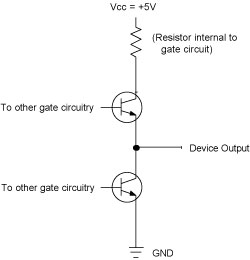
The output portion of a typical TTL IC contains two transistors, only one of which can conduct current at any time. These output transistors, as shown in Figure 1-5, internally connect the ICs output to 5V or to ground to produce a logic 1 or a logic 0 at the output.
Figure 1-5
The output of a typical TTL circuit includes two transistors than can switch the output between Vcc or GND to produce a logic 1 or a logic 0.
For clarity, this circuit shows only the output transistors, not the entire gate circuit.
To produce a logic 1 at its output, a TTL IC turns on the upper transistor, which allows current to flow from the 5V supply (V+, Vcc, or Vcc) through the output transistor to another circuit. The upper transistor provides a current source to the output, and the lower transistor provides a current-sink from the output to ground (GND).
A TTL input connected to this output will recognize a voltage between about 2.0V to 5.0V as a logic 1. The input will recognize a voltage between about 0.8V and 0.0V as a logic 0. Actual voltage ranges for inputs and outputs vary by logic families, as youll see later. The voltages noted above apply to the standard SN7400 family of ICs we use throughout this book.
The circuit in Figure 1-6a shows how a gate output sources current to produce a logic 1. (The diagram shows only the upper transistor and resistor from Figure 1-5.) Current flows from the power source, through the resistor, through the transistor, and through the LED, which lights up. When the IC produces a logic 0, the transistor turns off so no current can flow, and the LED turns off.
Figure 1-6a
The output of a standard TTL IC will source current when it produces a logic 1.
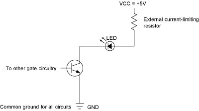
The circuit in Figure 1-6b illustrates how a gate output sinks current to produce a logic 0. (The diagram shows only the lower transistor from Figure 1-5.)
In this circuit, current flows from a power source through an LED to ground, so the LED lights whenever the TTL IC produces a logic 0. When the IC output changes to a logic 1, the transistor no longer conducts current, so the LED turns off. In this circuit, an external resistor in series with the LED limits current flow. The internal resistor shown in Figure 1-6a limits current in that circuit.
Figure 1-6b
The output of a standard TTL IC will sink current when it produces a logic 0. Although a standard TTL output may control an LED, other circuits better handle this task.
Buffers and drivers
A standard TTL device, such as an SN7400 NAND gate, can sink about 16 milliamperes (mA) and source about 1 mA. Although TTL devices can
operate small LEDs, good designers rely on special driver, or buffer, circuits to control real-world devices such as LEDs, motors, and relays.
A driver, often called a buffer, provides an output transistor designed specifically to operate high-current or high-voltage devices. Some manufacturers also produce drivers to control specific devices, such as stepper motors or displays.
The TTL family of ICs includes several devices with open-collector outputs that can drive low-current loads such as LEDs or small relays. The output circuit of an open-collector IC looks like the circuit shown previously in Figure 1-6b. The transistors collector terminal remains “open,” or unconnected to any other circuitry. When turned on, this transistor sinks current to ground, but it cannot source any current.
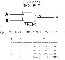
The circuit in Figure 1-7 shows a typical open-collector driver and its truth table. Note that only two logic-1 inputs to the SN7403 open-collector NAND gate cause
the IC to sink current. When the output does not conduct current to ground, it appears unconnected to external devices.
Figure 1-7
An open-collector output will act as either a disconnected (open) circuit or as a path to ground. Note that this diagram indicates the power and ground connections for the 74ALS03 IC.
Because an open-collector IC simply provides a “switch” that will connect a circuit to ground, an LED, relay, or resistor circuit must provide power. TTL ICs such as the SN7403 have specific current and voltage limits. Always check the data sheet for a device before you use it to drive any circuit outside its immediate logic “family.”
Special high-current open-collector devices described in Chapter 2 can drive loads that draw more current than the few tens of milliamperes a standard open-collector gate can handle.
Latches
All of the previous examples show simple gate circuits. As a gates inputs change, so does its output. But, logic circuits also rely on latches,
devices that take a “snapshot” of information and save it. A typical latch provides eight inputs and eight outputs. The eight inputs connect to a computer, and the eight outputs connect to drivers or other devices that require data to remain stable for long periods. Latches come in two varieties: level-sensitive and edge-sensitive.
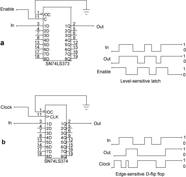
Figure 1-8a shows connections to a typical level-sensitive latch IC, the SN74LS373. (For clarity, the figure shows only one data signal.) As long as the ICs Enable signal remains at logic 1, an input signal (In) will pass through the latch to its corresponding output (Out). But, when the Enable signal becomes a logic 0, the latch snaps shut. Then the output remains as it was when the Enable signal changed from logic 1 to logic 0. In effect, the SN74LS373 IC acts like a small memory. Some designers refer to this type of latch as a transparent latch.
While the Enable signal remains at logic 0, the outputs remain latched. When the Enable signal changes to a logic 1, the In signal again passes directly through to the Out connection.
Figure 1-8a
A level-sensitive latch acts like a gate and lets signals pass through until it receives an Enable signal. Then, it “latches” and holds the
data, as long as Enable = 0.
Figure 1-8b
An edge-sensitive latch will update its data only on a transition of its Clock signal, in this case, a positive-going edge.
Figure 1-8b illustrates an edge-sensitive latch, the SN74LS374, also called an edge-sensitive D flip-flop. (For clarity, this figure also shows only one data signal.) This device transfers logic levels from its inputs to its outputs only at the instant its Clock signal changes from a logic 0 to a logic 1. The change, or edge, of the Clock signal causes the transfer to occur. The outputs remain stable until the next logic-0 to logic-1 transition, also called a positive-going edge. A logic-1 to logic-0 change, a negative-going edge, has no effect on the SN74LS374.
Latch circuits find use in many peripheral devices because they can “grab” data from a bus and hold the data until updated by a hardware signal, often generated
under software control. In this way, a computer can transfer data to external input/output (I/O) devices that youll learn more about later in this booklet.
Positive and negative logic
Some digital circuits require a logic 1 to cause an action, while other circuits require a logic 0. A level-sensitive latch closes when its Enable signal becomes a logic 0. On the other hand, in the open-collector driver circuit (see Figure 1-7), a logic 1 at both inputs causes the output to connect to ground.
When a circuit requires a logic 1 to operate, engineers may refer to this condition as positive logic. Thus, the more positive voltage causes the action to take place. On the other hand, if a circuit requires a logic 0 to cause action, this type circuit is referred to as negative logic.
Theres nothing “negative” or “positive” about these various circuits. The notation simply provides a shorthand that tells engineers and users whether a logic 1 or a logic 0 causes an action.
In the latch circuits shown in Figures 1-8a and 1-8b, each device has an Output Control signal, /OC, that connects to ground, or logic 0. These ICs provide three-state outputs and require a logic 0 at this input to enable the outputs to function. Because a logic 0 causes this action, you can think of the /OC input as a negative-logic input. The small circle on each /OC input indicates a logic 0 will cause the action described by the signal name. Also, signals that have a prefix “/” or a suffix “*”, such as START*, RESET*, or /END, often indicate a logic 0 causes the named action to occur.
All in the family
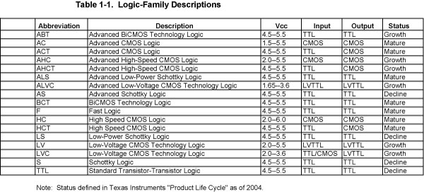
The TTL family tree now includes many varieties of logic circuits, from the plain-vanilla SN74xx TTL series of ICs to newer ICs aimed at high-speed, low-power designs. Table 1-1 lists several of the most widely used families of logic devices, but other families also exist. The notations “growth”, “mature”, and “decline” used in Table 1-1 simply refer to the type of market for these devices.
Table 1-1
Logic-Family Descriptions
Check the Texas Instruments (Dallas, TX) Web site at www.ti.com for current information about logic families and characteristics. Look under Digital Logic > About Logic > Logic Selection Guide.
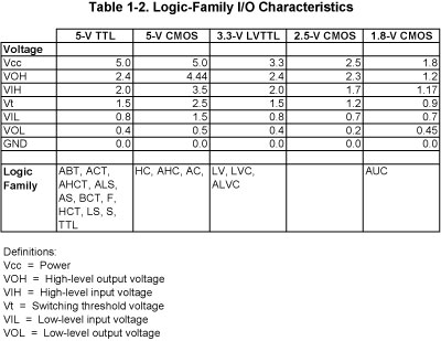
Logic families involve several technologies ranging from bipolar semiconductors in the older families to hybrid bipolar-CMOS devices (BiCMOS), and CMOS-only devices. The type of technology will affect the operation of devices as well as their supply voltages, current-sink and current-source capabilities, and operating speed. Each family of
devices has its own specifications for voltage outputs and inputs as shown in Table 1-2.
Chapter Notes
1. Boolean logic operations got their name from George Boole (1815-1864), a self-taught British mathematician. In 1854, Boole published a book that established an algebraic way of thinking about logic and about logical operations such as AND, OR, and NOT. Booles algebra provides the basis for all digital circuits.
For more information
We hope you found the Chapter 1 informative. To go back to the Main Page click here.
You can purchase the complete Digital I/O Handbook for only $19.95 by clicking here. The Digital I/O Handbook is FREE with any qualifying Sealevel Digital I/O product purchase.

